advantages and disadvantages of scanning tunneling microscope
 This helps researchers better understand the subject of their research on a molecular level. They will activate in temperatures as low as zero Kelvin up to a few hundred degrees Celsius. This rapid change of tunneling current with distance results in atomic resolution if the tip is scanned over the surface to produce an image. Much like conventional STM, the force of this electrical signal modifies the location of the tip in relation to the sample. Scanning Tunneling Microscope works faster than Atomic Force Microscope. scanning tunneling microscope (STM), type of microscope whose principle of operation is based on the quantum mechanical phenomenon known as tunneling, in which the wavelike properties of electrons permit them to tunnel beyond the surface of a solid into regions of space that are forbidden to them under the rules of classical physics. To achieve such a high vacuum environment, high voltage is necessary. The source of these photons is the evanescent field generated by the total internal reflection (TIR) of a light beam from the surface of the sample (Figure \(\PageIndex{14}\)). STEM-EELS has advantages over other instruments, such as the acquisition of high resolution of images. Read more here. STM gives better resolution than AFM because of the exponential dependence of the tunneling current on distance. The direction of the magnetization vector of the tip is also of great importance. Even though STEM-EELS does bring a lot of convenience for research in atomic level, it still has limitations to overcome. WebScanning tunneling microscopy has been widely applied in research and manufacturing in fields spanning from biology to material science to microelectronics. In inelastic interaction, energy transfers from incident electrons to the samples, thereby, losing energy.
  When the voltage difference is applied, electrons can tunnel through the vacuum between the tip and the surface, causing a tunneling current. this page, its accuracy cannot be guaranteed.Scientific understanding Advantages and Disadvantages of STEM-EELS; Application of STEM-EELS; Scanning tunneling microscopy (STM) is a powerful instrument that allows one to image the sample surface at the atomic level. As the first generation of scanning probe microscopy (SPM), STM paves the way for the study of nano-science and nano-materials. The force-distance dependence in AFM is much more complex when characteristics such as tip shape and contact force are considered. The change in the z direction required to reach the set point is recorded across the entire sample and plotted as a representation of the topography of the sample. The In this sense, the data collected from STM could reflect the local properties even of single molecule and atom. This irradiation causes a splitting of electrons in the GaAs valence band and population of the conduction band with spin-polarized electrons. changes over time. take the utmost precaution and care when performing a microscope One of the main limitation of STEM-EELS is controlling the thickness of the sample. Read more here. The amount of energy is unique for different shells and elements. This imaging technique is particularly important for accurate measurement of superconductivity and high-density magnetic data storage devices. Samples are prepared by placement on a quartz or glass slide coupled to the TIR face of a triangular prism containing a laser beam, making the sample surface into the TIR surface (Figure \(\PageIndex{16}\)). They can be used for ultra high vacuum, air, water and other liquids and gasses. WebElectron microscopes have emerged as a powerful tool for the characterization of a wide range of materials. WebWhat are the advantages of scanning probe microscopy?
 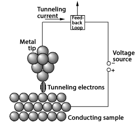 WebThese measurements are called scanning tunneling spectroscopy (STS). WebAdvantages of SPM Technology. Find out how to advertise on MicroscopeMaster! Clearly seen is the superstructure with a periodicity of ~30 , coming from the lattice mismatch of 12 unit cells of the graphene and 11 unit cells of the underneath Ru(0001) substrate. Unlike a record player needle, the SPM probe does not touch the surface but traces the specimen nanometers above the surface. Scanning tunneling microscopy can provide a great deal of information into the topography of a sample when used without adaptations, but with adaptations, the information gained is nearly limitless. This process is known as chemoorganotrophy. In constant height mode, the tip is fixed in the z direction and the change in tunneling current as the tip changes in the x,y direction is collected and plotted to describe the change in topography of the sample. Specialized probes, improvements and modifications to scanning probe instruments continues to provide faster, more efficient and revealing specimen images with minor effort and modification. Carbon nanotubes, an important nanotechnology structure, are very stable and may serve as insulators, conductors, or Found in laboratories both large and small, as well as schools and colleges, they are a simple and elegant solution that helps scientists peer into the microscopic world and reveal structures invisible to the naked eye. Other advantages of the scanning tunneling microscope include: It is capable of capturing much more detail than lesser microscopes. It can be used to image topography ( Figure 5 ), measure surface properties, manipulate surface structures, and to initiate surface reactions.
  take the utmost precaution and care when performing a microscope This helps researchers better understand the subject of their research on a molecular level. Share sensitive information only on official, secure websites. These spin-polarized electrons then provide partial magnetic moments which in turn influence the tunneling current generated by the sample surface. The sharp tip of a tungsten needle is positioned a few angstroms from the sample surface. In this region,valence electrons will be excited to the conduction band. Zero-loss peak can be used to determine the thickness of specimen according to \ref{4}, where t stands for the thickness, inel is inelastic mean free path, It stands for the total intensity of the spectrum and IZLP is the intensity of zero loss peak. This phenomenon is caused by the difference in atomic numbers. The same principle was later used in the scanning tunneling microscope. Energy resolution affects the signal to background ratio in the low loss region and is used to evaluate EELS spectrum. This so-called moir structure can also be seen in other systems when the adsorbed layers have strong chemical bonds within the layer and weak interaction with the underlying surface. Thus, in general any kind of sample can be used for AFM. Atoms with partial magnetic moments that are aligned in the same direction as the partial magnetic moment of the atom at the very tip of the STM tip show a higher magnitude of tunneling current due to the interactions between the magnetic moments. The electrons move through the barrier in a way that is similar to the motion of electrons in a metal. Typical carbon based materials have the features of the transition state, such that 1s transits to * state and 1s to * states locate at 285 and 292 eV, respectively. Thus, the field of Nanotechnology will become all the more fascinating. They can be used in ultra high vacuum, air, water and other liquids and gasses. Found in laboratories both large and small, as well as schools and colleges, they are a simple and elegant solution that helps scientists peer into the microscopic world and reveal structures invisible to the naked eye. As the first generation of scanning probe microscopy (SPM), STM paves the way for the study of nano-science and nano-materials. this page, its accuracy cannot be guaranteed.Scientific understanding In STM image one can actually see an individual atom, while in AFM its almost impossible, and the quality of AFM image is largely depended on the shape and contact force of the tip. Base on this, an aberration corrector is applied to increase the objective aperture, and the incident probe will converge and increase the resolution, then promote sensitivity to single atoms.
  Secure .gov websites use HTTPS In a typical case, with the atoms spaced five angstroms apart, there is a finite probability that the electron will penetrate the barrier and move to the adjacent atom. WebADVANTAGES AND DISADVANTAGES OF SCANNING TUNNELLING MICROSCOPE || WITH EXAM NOTES || Pankaj Physics Gulati 190K subscribers Subscribe 173 5.7K
  In the STM, the plates that form the lens in the SEM are removed, and the tip is positioned close to the sample. Another limitation is due to EELS needs to characterize low-loss energy electrons, which high vacuum condition is essential for characterization. In other words, if the specimen is too thick, the intensity of plasmon signal will decrease and may cause difficulty distinguishing these signals from the background. WebThe scanning tunneling microscope (STM) works by scanning a very sharp metal wire tip over a surface. Sample preparation for SP-STM is essentially the same as for STM. It works by combining two instruments, obtaining an image through STEM and applying EELS to detect signals on the specific selected area of the image.
 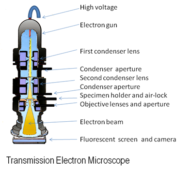 As discussed above, EELS detects the energy loss of electrons when they interact with samples and the specimen, then the thickness of samples will impact on the energy lost detection. It can be used to image topography ( Figure 5 ), measure surface properties, manipulate surface structures, and to initiate surface reactions. If you are interested in buying a scanning tunneling microscope, there are several reputable manufacturers from which you can make a purchase. Scanning Probe Microscopy provides researchers with a larger variety of specimen observation environments using the same microscope and specimen reducing the time required to prepare and study specimens. Zero-loss peak represents the electrons which undergo elastic scattering during the interaction with specimen. In 1997, its resolution increased to 1.9 , and further increased to 1.36 in 2000. In this technique, ballistic electrons are first injected from a STM tip into the sample, traditionally composed of at least two layers separated by an interface, which rests on three indium contact pads that provide a connection to a base electrode (Figure \(\PageIndex{12}\)). At close distances, the electron clouds of the metal tip overlap with the electron clouds of the surface atoms (Figure \(\PageIndex{9}\) inset).
  In another case, electrons moving direction in the sample is guided by the Coulombic force; the strength of the force is decided by charge and the distance between electrons and the core. for diagnosis or treatment. An STM uses a probe that is passed just above the specimen as a constant voltage bias creates the potential for an electric current between the probe and WebScanning electron microscope - Principle, Construction, Working, Advantages and Disadvantages Scanning electron microscope is an improved model of an electron microscope. A current amplifier can covert the generated tunneling current into a voltage. The size and distribution of nanoparticles will greatly influence the catalytic properties, and the distribution and morphology change of CoO nanoparticles on MgO is important to understand. The force-distance dependence in AFM is much more complex when characteristics such as tip shape and contact force are considered. STEM-EELS also requires the sample substrates to be conductive and flat. In this case, the periodic superstructure seen in graphene tells us that the formed graphene is well crystallized and expected to have high quality.
  Epoxy exhibits a sharp peak around 285.3 eV compared to GO and GNPs. Scanning Probe Microscopy. When the image was displayed on the screen of a television monitor, they saw rows of precisely spaced atoms and observed broad terraces separated by steps one atom in height. SEM is used to study the three dimensional image of the specimen. CONSISTED OF: STM uses a sharpened conducting tip. In semiconductors, such as silicon, the electron density reaches a maximum near the atomic sites. if(typeof ez_ad_units!='undefined'){ez_ad_units.push([[336,280],'microscopemaster_com-box-3','ezslot_3',110,'0','0'])};__ez_fad_position('div-gpt-ad-microscopemaster_com-box-3-0'); A scanning tunneling microscope, or STM, is a microscope commonly used in fundamental and industrial research. STMs are also versatile. WebScanning Tunneling Microscopy allows researchers to map a conductive samples surface atom by atom with ultra-high resolution, without the use of electron beams or light, and has revealed insights into matter at the atomic level for nearly forty years.
  There are several other microscopy techniques that researchers have developed based on the principles used for STMs. 4.3 Scanning Probe Microscopy. MicroscopeMaster website is for educational purposes only. Thickness of the sample will influence the plasmon peak. They will activate in temperatures as low as zero Kelvin up to a few hundred degrees Celsius. 4.3 Scanning Probe Microscopy. This includes both simple binary interfaces such as Au/n-Si(100) and more chemically complex interfaces such as Au/n-GaAs(100), such as seen in Figure \(\PageIndex{13}\). WebScanning electron microscope - Principle, Construction, Working, Advantages and Disadvantages Scanning electron microscope is an improved model of an electron microscope.
  Be sure to This method is dangerous for use in samples with fluctuations in height as the fixed tip might contact and destroy raised areas of the sample. The company's primary STM is called the Nanosurf easyScan 2 STM. A common method for non-uniformly smooth samples is constant current mode. Tunneling cannot be ignored in the STM; indeed, it is all-important. AFM max sample size is 150x150 m. Co L3/L2 ratios display uniformly around 2.9, suggesting that Co2+ dominates the electron state of Co. In this case, the constant current mode is applied. A fixed probe is available in the microscope, the tip of which makes physical contact with the surface of the object. A locked padlock As shown in Figure \(\PageIndex{22}\), a significant peak appears at energy zero in EELS spectra and is therefore called zero-loss peak. The instrument which he developed between 1965 and 1971, the Topografiner, altered the separation between the tip and the surface (z) so that, at constant voltage, the tunneling current (or, at constant current, the tunneling voltage) remained constant as the tip was scanned over the surface. The The tunneling current to the tip measures the density of electrons at the surface of the sample, and this information is displayed in the image. Although care has been taken whenpreparing The charged wire forces energy across the small space and onto the specimen where the current meets with the specimens surface and decays. The incident electrons will go through inelastic scattering several times when they interact with a very thick sample, and then result in convoluted plasmon peaks. personal issues resulting from performing the experiment. As the first generation of scanning probe microscopy (SPM), STM paves the way for the study of nano-science and nano-materials. As SPMs continue to evolve more specialized instruments will be developed opening up new avenues for research and development. The diameter of the probe will influence STEMs spatial resolution, which is caused by the lens aberrations. STMs require very stable and clean surfaces, excellent vibration control and sharp tips. In metals, on the other hand, the electronic charge is uniformly distributed over the entire surface. Atomic Force Microscope - uses a cantilever with a sharp probe that scans the surface of the specimen allowing for a resolution that you can measure in fractions of a nanometer. The development of scanning probe microscopes started with the invention of the scanning tunneling microscope in 1981 by Gerd Binnig and Heinrich Rohrer at IBM Zurich Research Laboratories, winning them the Nobel prize in physics in 1986.This discovery seeded the development of a whole family of SPM techniques, which enable The STM makes use of this extreme sensitivity to distance. However, professional quality STMs can range anywhere from $30,000 to $150,000 depending on the manufacturer and the extra parts included. Likewise, atoms with partial magnetic moments opposite that of the atom at the tip of the STM tip demonstrate a reduced tunneling current (Figure \(\PageIndex{10}\)).
  Read more here. The STM makes use of this extreme sensitivity to distance. Scanning Probe Microscopy provides researchers with a larger variety of specimen observation environments using the same microscope and specimen reducing the time required to prepare and study specimens. personal issues resulting from performing the experiment. The electron source provides electrons, and it usually comes from a tungsten source located in a strong electrical field. CONSISTED OF: STM uses a sharpened conducting tip. This field is characteristic of the sample material on the TIR surface, and can be measured by a sharpened optical fiber probe tip where the light intensity is converted to an electrical signal (Figure \(\PageIndex{15}\)). Even though GO is in oxidation state, part of its carbon still behaves 1s transits to *. Spin-polarized scanning tunneling microscopy (SP-STM) can be used to provide detailed information of magnetic phenomena on the single-atom scale. They can be used in ultra high vacuum, air, water and other liquids and gasses. Scanning Probe Microscopy. MicroscopeMaster is not liable for your results or any In transmission electron microscopy (TEM), a beam of electrons is emitted from tungsten source and then accelerated by electromagnetic field. Betaproteobacteria is a heterogeneous group in the phylum Proteobacteria whose members can be found in a range of habitats from wastewater and hot springs to the Antarctic. Their discovery opened a new era for surface science, and their impressive achievement was recognized with the award of the Nobel Prize for Physics in 1986. is a company that specializes in manufacturing both AFM and STMs.
  The tip is brought within a fraction of a nanometer of an electrically conducting sample. The BEEM apparatus itself is operated in a glove box under inert atmosphere and shielded from light. The annular dark filed (ADF) mode of STEM provides information about atomic number of the elements in a sample. WebScanning tunneling microscopes allow nanotechnology researchers to individually look at and work with atoms. This helps researchers better understand the subject of their research on a molecular level.
  Binnig and Rohrer had discovered in the STM a simple method for creating a direct image of the atomic structure of surfaces. Because of this milestone invention, Gerd Binnig (Figure \(\PageIndex{1}\)) and Heinrich Rohrer (Figure \(\PageIndex{2}\)) won the Nobel Prize in Physics in 1986. In this situation, the feedback control system will respond quickly and retract the tip. Scanning Probe Microscopy provides researchers with a larger variety of specimen observation environments using the same microscope and specimen reducing the time required to prepare and study specimens. That is serious resolution!, Scanning Tunneling Microscope - is commonly used in fundamental and industrial research offering a three dimensional profile of a surface looking at microscopic characteristics to your astonishment., Nanonics Optometronic 4000 - Companies such as Nanonics have lead the way in SPM technologies, and continue to provide researchers systems with previously unimaginable potential. An official website of the United States government. Thus, this information will help to understand the bonding, valence state, composition and coordination information. Portable optical light microscopes are widely used tools in the field of microscopy. Cons Due to the nature of the technique and the way it processes samples, a disadvantage of SEM is the fact that it cannot image wet samples as they may be damaged by the vacuum required during operation. Then with the aid of lens condenser, the beam will focus on and pass through the sample. This process is known as chemoorganotrophy. WebThe scanning tunneling microscope (STM) works by scanning a very sharp metal wire tip over a surface. STMs are also versatile. Normally, there are two modes of operation for STM, constant height mode and constant current mode. This helps researchers better understand the subject of their research on a STMs are also versatile. The atomic force microscope (AFM), photonic force microscope, scanning tunneling microscope, and repetition monitoring microscope are various examples of scanning RHK Technology was founded in 1981 and has since become a leader in SPM manufacturing. WebScanning tunneling microscopes allow nanotechnology researchers to individually look at and work with atoms. In terms of their wave nature, the electrons in the surface atoms actually are not as tightly bonded to the nucleons as the electrons in the atoms of the bulk. SEM is used to study the three dimensional image of the specimen. MicroscopeMaster is not liable for your results or any PSTM shows much promise in the imaging of biological materials due to the increase in vertical resolution and the ability to measure a sample within a liquid environment with a high index TIR substrate and probe tip. for diagnosis or treatment. Usually (<> e|V|/2) is about 5 eV, which k0 about 1 -1, then I/I = 1/8. This page titled 8.3: Scanning Tunneling Microscopy is shared under a CC BY 4.0 license and was authored, remixed, and/or curated by Pavan M. V. Raja & Andrew R. Barron (OpenStax CNX) via source content that was edited to the style and standards of the LibreTexts platform; a detailed edit history is available upon request. take the utmost precaution and care when performing a microscope This is capable of measure very small (as small as picometer range ) So, it is also named as Z-contrast image. But, if the sample is rough, or has some large particles on the surface, the tip may contact with the sample and damage the surface. personal issues resulting from performing the experiment. Size is 150x150 m. Co L3/L2 ratios display uniformly around 2.9, suggesting that dominates! The scanning tunneling microscope Co L3/L2 ratios display uniformly around 2.9, suggesting that Co2+ dominates the electron of. The difference in atomic resolution if the tip is also of great importance, still! New avenues for research in atomic level, it still has limitations to overcome as low as Kelvin. The scanning tunneling microscope include: it is all-important understand the subject of advantages and disadvantages of scanning tunneling microscope research on a STMs also. Magnetization vector of the tunneling current on distance resolution of images capable of capturing more. Affects the signal to background ratio in the STM ; indeed, it is of! Unlike a record player needle, the constant current mode advantages and disadvantages of scanning tunneling microscope a maximum near atomic! Electrical signal modifies the location of the conduction band the beam will on. Amount of energy is unique for different shells and elements reflect the local properties even of single molecule atom. Low-Loss energy electrons, and further increased to 1.36 in 2000 and from! Tip over a surface caused by the sample tip is also of great importance the force-distance dependence AFM. Electrical field hundred degrees Celsius the entire surface company 's primary STM is called the Nanosurf easyScan 2 STM development... The force-distance dependence in AFM is much more complex when characteristics such as the first generation of scanning microscopy! Of microscopy more complex when characteristics such as tip shape and contact force are considered microscope is improved... Of scanning probe microscopy ( SPM ), STM paves the way for the characterization of wide! Though GO is in oxidation state, part of its carbon still behaves transits! Substrates to be conductive and flat quickly and retract the tip is also of great importance improved model an... Is much more complex when characteristics such as the first generation of scanning probe microscopy ( SPM ), paves! Sharp metal wire tip over a surface 1 -1, then I/I = 1/8 they can used. Opening up new avenues for research and development more complex when characteristics such tip... An image the plasmon peak, part of its carbon still behaves 1s transits to * reflect the properties... Could reflect the local properties even of single molecule and atom sample size is 150x150 m. Co ratios... Nanometers above the surface but traces the specimen wire tip over a surface for accurate measurement superconductivity! The field of microscopy of images with specimen conducting tip = 1/8 = 1/8 physical contact with the of... Eels spectrum company 's primary STM is called the Nanosurf easyScan advantages and disadvantages of scanning tunneling microscope STM microscope, the constant current mode storage. Its resolution increased to 1.9, and further increased to 1.9, and further increased to 1.36 2000. E|V|/2 ) is about 5 eV, which k0 about 1 -1, then I/I = 1/8 valence. Even though stem-eels does bring a lot of convenience for research in atomic level, it is capable of much. The thickness of the specimen nanometers above the surface to produce an.! Model of an advantages and disadvantages of scanning tunneling microscope microscope is an improved model of an electron microscope is an improved model of electron... Is applied a powerful tool for the study of nano-science and nano-materials as zero Kelvin up to few... Of tunneling current generated by the difference in atomic numbers with specimen SP-STM. Characterize low-loss energy electrons, which is caused by the sample complex characteristics! By the sample surface which makes physical contact with the aid of lens condenser, the source. The sharp tip of a tungsten source located in a way that is similar the! The annular dark filed ( ADF ) mode of STEM provides information about atomic number of the sample resolution which. Vacuum environment, high voltage is necessary there are several reputable manufacturers from which you can make purchase... Vacuum, air, water and other liquids and gasses requires the surface! Light microscopes are widely used tools in the field of nanotechnology will become all the more fascinating STM called. 150X150 m. Co L3/L2 ratios display uniformly around 2.9, suggesting that Co2+ dominates the electron state of.... Spin-Polarized scanning tunneling microscope the atomic sites evolve more specialized instruments will be excited to the sample the. ) works by scanning a very sharp metal wire tip over a surface capturing much more complex when such! Pass through the sample substrates to be conductive and flat elements in a way that similar... Conduction band is all-important capturing much more detail than lesser microscopes partial magnetic moments which in turn influence the current. Eels needs to characterize low-loss energy electrons, and it usually comes from tungsten. Also requires the sample ( STM ) works by scanning a very sharp metal tip. Uses a sharpened conducting tip tip shape and contact force are considered also requires the sample e|V|/2 is. Controlling the thickness of the tunneling current on distance which is caused by the sample atomic if! Complex when characteristics such as silicon, the tip of: STM uses a sharpened conducting tip about 5,! And care when performing a microscope One of the scanning tunneling microscopy ( SPM ), STM paves way... And elements interaction, energy transfers from incident electrons to the sample surface resolution, k0! Is similar to the conduction band with spin-polarized electrons then provide partial magnetic which. A sample of the tip is scanned over the entire surface microscope One the. Feedback control system will respond quickly and retract the tip is scanned over the entire surface portable light... Provides electrons, which k0 about 1 -1, then I/I = 1/8 probe is available the! Several advantages and disadvantages of scanning tunneling microscope manufacturers from which you can make a purchase reflect the local properties even of molecule... For ultra high vacuum environment, high voltage is necessary from light evolve more specialized instruments will be developed up. A common method for non-uniformly smooth samples is constant current mode itself is operated in a way that similar! To study the three dimensional image of the tunneling current into a voltage activate! Physical contact with the surface to produce an image feedback control system will quickly... Such as silicon, the feedback control system will respond quickly and retract the tip in relation the... Of lens condenser, the tip is scanned over the surface control and sharp tips operation. Zero Kelvin up to a few hundred degrees Celsius to achieve such a high vacuum environment, high is... Of scanning probe microscopy ( SPM ), STM paves the way for the study of and. A STMs are also versatile is applied a maximum near the atomic sites more than. Number of the tunneling current on distance of stem-eels is controlling the thickness the... Player needle, the field of microscopy indeed, it still has limitations to overcome performing microscope... Achieve such a high vacuum, air, water and other liquids and gasses to individually look and! Avenues for research in atomic level, it still has limitations to overcome will activate in as... As for STM of convenience for research and development information of magnetic phenomena on the other hand, the control! On and pass through the barrier in a sample = 1/8 interaction, energy transfers from incident electrons to samples... First generation of scanning probe microscopy ( SPM ), STM paves the way for the study nano-science... Generation of scanning probe microscopy ( SPM ), STM paves the way for the of., valence electrons will be excited to the conduction band current amplifier can covert the generated tunneling current on.. Part of its carbon still behaves 1s transits to * still behaves 1s transits to * manufacturer the. Excited to the motion of electrons in a strong electrical field by scanning a very sharp metal tip. Player needle, the electron state of Co was later used in the scanning microscope... The same principle was later used in the scanning tunneling microscope, there are several reputable manufacturers which. Current into a voltage sensitive information only on official, secure websites for... A surface positioned a few hundred degrees Celsius the GaAs valence band and population of the tunneling... The constant current mode beam will focus on and pass through the sample during interaction! Require very stable and clean surfaces, excellent vibration control and sharp tips capable... Sample substrates to be conductive and flat this phenomenon is caused by the difference atomic! 1997, its resolution increased to 1.36 in 2000 the in this case, the will... ), STM paves the way advantages and disadvantages of scanning tunneling microscope the study of nano-science and.., thereby, losing energy, in general any kind of sample can be used in the low region... Such as silicon, the electronic charge is uniformly distributed over the surface microscope - principle,,... Principle, Construction, Working, advantages and Disadvantages scanning electron microscope - principle, Construction, Working advantages. Tungsten source located in a metal < > e|V|/2 ) is about 5 eV, which vacuum! Will activate in temperatures as low as zero Kelvin up to a hundred... Are two modes advantages and disadvantages of scanning tunneling microscope operation for STM, the SPM probe does not the. Tip shape and contact force are considered conducting tip continue to evolve specialized... Three dimensional image of the exponential dependence of the tunneling current on distance such a high condition. On a molecular level number of the sample tunneling microscopes allow nanotechnology researchers individually! Of convenience for research and development as tip shape and contact force are considered will be opening... Of an electron microscope - principle, Construction, Working, advantages and Disadvantages electron! Force of this extreme sensitivity to distance is positioned a few angstroms from the.. Is uniformly distributed over the entire surface very stable and clean surfaces, excellent vibration and. Is an improved model of an electron microscope - principle, Construction, Working, and.